


Subscribe To Get Information, Latest News And Other Interesting Events!


Important Links
Get In Touch
Ariston Publication
3167 Riverview Place
Columbus, OH 43202
United States of America
Copyright © 2026 Ariston Publications. All Rights Reserved.
Loading Your Library
Preparing your reading experience...
Loading content...
Ariston Publication
3167 Riverview Place
Columbus, OH 43202
United States of America
Bishal Hazarika, K Bijayata Singha, Sagar Bhattarai
Bishal Hazarika1
K Bijayata Singha1
Sagar Bhattarai2,3*
1 Department of Physics, Cotton University, Panbazar, Guwahati 781001, Assam, India
2 Department of Physics, Cotton University, Panbazar, Guwahati 781001, Assam, India
3Technology Innovation Hub, Indian Institute of Technology Guwahati, Guwahati 781039, Assam, India
*Author to whom correspondence should be addressed:
sagarbhattarai012@gmail.com (S. Bhattarai)
In this study, the photovoltaic performance of CdTe based thin-film solar cells with an IGZO electron transport layer (ETL) and Cu2O hole transport layer (HTL) is studied through SCAPS-1D simulation software. In order to improve the performance of the cell, variations in absorber thickness, defect densities in ETL (IGZO) and HTL(Cu2O), and different choices for front and rear contacts were examined. It is clear from the simulation results that variation in any of these factors plays a vital role in improving the power conversion efficiency (PCE), open-circuit voltage (Voc ), short-circuit current density (Jsc ), and fill factor (FF). The most significant factor in improving efficiency turned out to be the absorber's defect density, followed by selecting good contact materials. The maximum efficiency achieved via simulations gives values of 18.84 mA/cm2 for Jsc . 1.35 V for Voc , 90.46% for FF, and PCE of 23.01% under AM1.5G radiation.
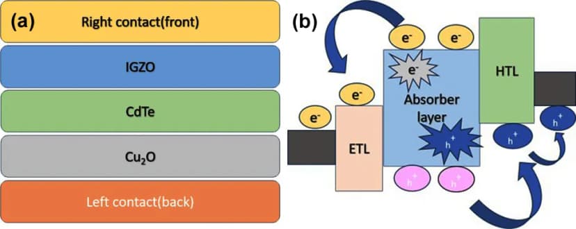
This study is significant because it systematically demonstrates, through SCAPS-1D simulation, how key physical and interfacial parameters govern the photovoltaic response of CdTe-based thin-film solar cells employing IGZO as the electron transport layer and Cu2O as the hole transport layer. Its novelty lies in the combined optimization of absorber thickness, defect densities in the transport layers, and front/rear contact selection within a single device architecture, enabling clear identification of the dominant loss mechanisms and performance-limiting factors. Scientifically, the work highlights the critical influence of absorber defect density and contact engineering on suppressing recombination and improving charge extraction, thereby enhancing power conversion efficiency, open-circuit voltage, short-circuit current density, and fill factor. The key contribution is the provision of a simulation-guided optimization pathway that yields a maximum PCE of 23.01% under AM1.5G illumination, along with improved Jsc, Voc, and FF. These findings are relevant for the design and development of higher-efficiency CdTe-based thin-film photovoltaic devices and may inform future experimental fabrication and device engineering strategies.
The study used SCAPS-1D to simulate CdTe-based thin-film solar cells with IGZO as the ETL and Cu2O as the HTL. It investigated how absorber thickness, defect densities in the transport layers, and front/rear contact materials affect device performance. The results showed that these parameters strongly influence PCE, Voc, Jsc, and FF, with absorber defect density having the greatest impact, followed by contact selection. The optimized device achieved 18.84 mA/cm² Jsc, 1.35 V Voc, 90.46% FF, and 23.01% PCE under AM1.5G illumination.
Article type: Research Article
Submitted: 21 May 2026
Revised: 2 August 2026
Accepted: 12 August 2026
First published: 29 August 2026
DOI: https://doi.org/10.69626/sop.2026.0044
Volume: 01
Issue: 01
Pages: 44-57
Citation: Science of Optics and Photonics 1(1), 44-57 (2026)
Hazarika, B., Singha, K.B. and Bhattarai, S. 2026. Novel Combined Strategy to Obtain More Efficiency in the CdTe – Thin Film Solar Cell using SCAPS – 1D. Science of Optics and Photonics 1(1), pp. 44-57; https://doi.org/10.69626/sop.2026.0044.
Number of downloads: 0
Number of views: 1